TSMC to start using High-NA EUV lithography in 2030 — A10 or A11 technology prime candidates for use
⚡ Quick Hits
**
- TSMC targets 2030 for its official High-NA EUV lithography rollout.
- The ultra-advanced A10 or A11 manufacturing nodes are the prime candidates for this technology.
- This calculated timeline sets the stage for the next major leap in global semiconductor performance.
**
**
Greetings, tech seekers! The Tech Monk is here to decipher the latest whispers from the silicon foundries. If you are wondering what the future of ultra-fast, highly efficient computing looks like, the roadmaps are finally starting to clear up.
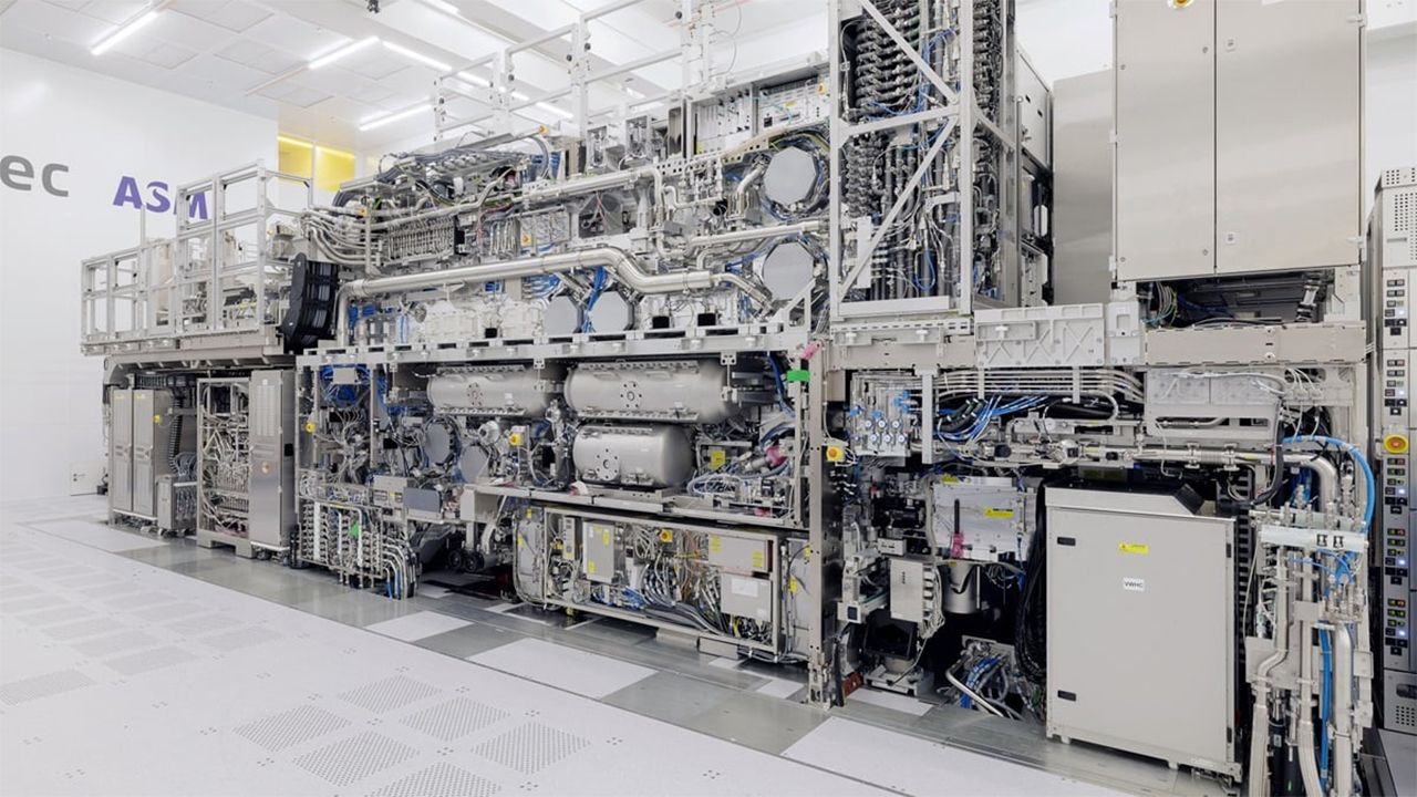
According to the latest industry murmurs—closely tracked by veteran semiconductor journalists like Anton Shilov—semiconductor titan TSMC is officially eyeing 2030 to begin utilizing High-NA (High Numerical Aperture) EUV lithography. This massive, next-generation manufacturing equipment is the key to shrinking transistors down to near-atomic levels, allowing for unprecedented processing power and energy efficiency.
While TSMC has been taking a measured, patient approach to acquiring these complex machines compared to some of its rivals, their target is now coming into focus. The prime candidates for this High-NA EUV integration will be TSMC's future A10 or A11 technology nodes.
By waiting until the A10/A11 generation at the end of the decade, TSMC is aiming to ensure that the transition to High-NA EUV is not only technologically sound but economically viable for the tech giants who rely on their fabrication plants. Prepare your gear—the 2030s are already shaping up to be a golden era for PC, smartphone, and AI hardware!