Chinese startup claims photonic chip production without DUV lithography, says nanoimprint process cuts costs by 90% — 8-inch wafers produced without conventional optical lithography
⚡ Quick Hits
- Replaces expensive, conventional DUV optical lithography with a nanoscale imprint technique.
- The alternative manufacturing process reportedly reduces production costs by up to 90%.
- Marks a significant milestone with the successful production of 8-inch photonic wafers.
Greetings, tech enthusiasts! The Tech Monk here, bringing you a fascinating development from the ever-evolving semiconductor landscape. While the global industry continues to battle over access to wildly expensive, highly complex lithography equipment, a Chinese startup has just thrown a massive curveball into the mix.
According to recent industry reports, this startup claims to have achieved a manufacturing breakthrough by successfully producing 8-inch photonic wafers. The most compelling part of this story? They completely bypassed conventional Deep Ultraviolet (DUV) optical lithography.
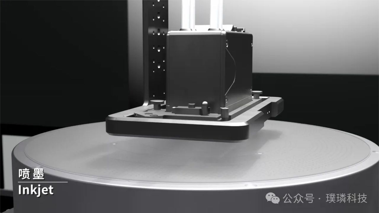
Instead of relying on complex light-based etching machines, the company utilized a cutting-edge nanoimprint process. By essentially "stamping" the nanoscale patterns directly onto the silicon, they have reportedly slashed manufacturing costs by an incredible 90%.
If these claims hold true at scale, this could be a revolutionary stepping stone for the hardware industry. Photonic chips—which use light instead of traditional electrical signals to process and transfer data—are poised to be the backbone of next-generation, hyper-efficient computing. Finding a way to produce them at a fraction of the traditional cost could vastly accelerate their adoption in the market. As always, I'll be keeping a close eye on whether this nanoimprint technology can truly scale up to meet commercial demand. Stay tuned!