Intel becomes the first company to ship high-volume logic chips made with ASML's High NA EUV — select Panther Lake layers on 18A are now dual-qualified for 0.55 NA scanners
⚡ Quick Hits
- Intel is the first manufacturer to ship high-volume logic chips using ASML's High NA EUV technology.
- Specific layers of the upcoming Panther Lake chips are now dual-qualified for 0.55 NA scanners on the 18A node.
- This manufacturing leap secures Intel a critical competitive edge in next-generation semiconductor lithography.
Greetings, tech disciples! The Tech Monk here, bringing you a monumental update straight from the silicon foundries.
If you've been tracking the intense race for smaller, more power-efficient semiconductor nodes, Intel has just pulled ahead in a critical category. The tech giant has officially become the very first company to ship high-volume logic chips manufactured using ASML's groundbreaking High NA (Numerical Aperture) EUV lithography.
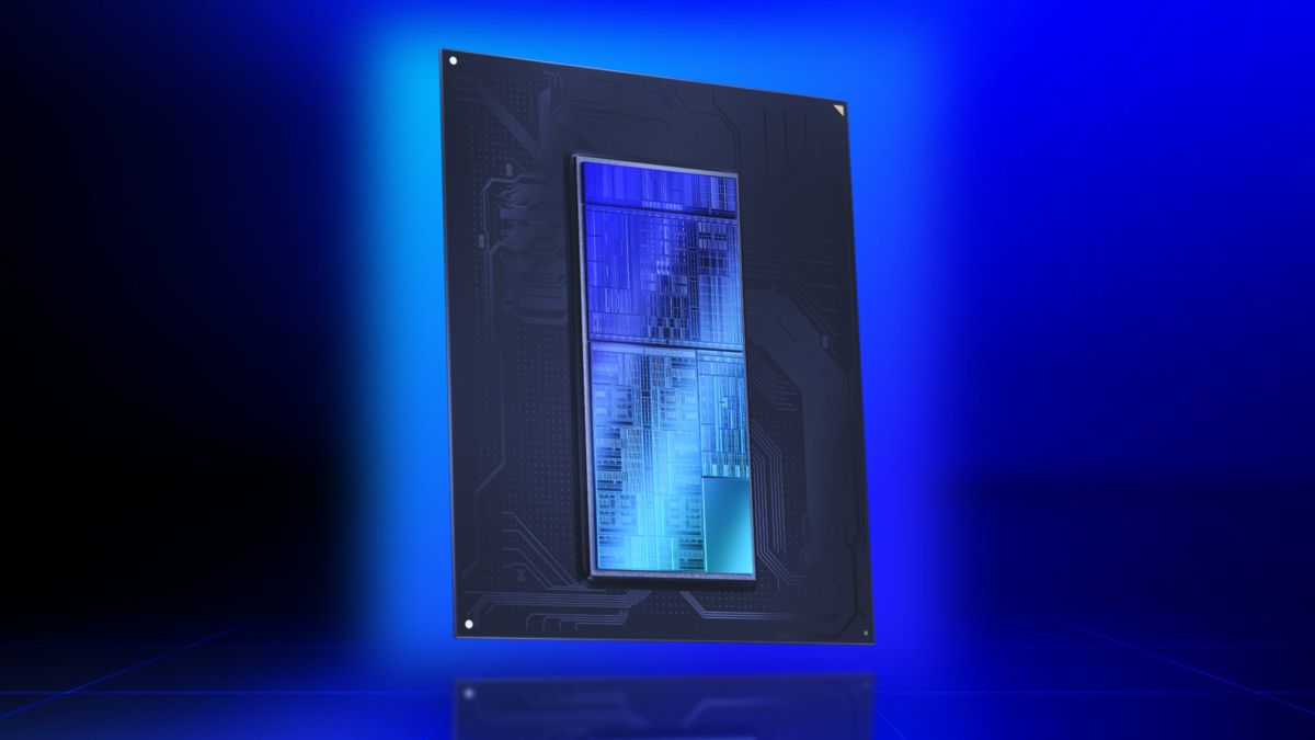
Specifically, select layers of Intel's highly anticipated Panther Lake processors, built on the advanced 18A node, are now dual-qualified for 0.55 NA scanners. This means Intel is no longer just experimenting in the lab with next-generation lithography—they are actively deploying it for commercial scale.
Why does this matter to us? ASML's High NA EUV machines allow chipmakers to print significantly smaller, denser features on silicon wafers. This translates directly to faster, more power-efficient processors for everything from enterprise AI servers to your next high-performance laptop. By conquering the 0.55 NA scanner qualification, Intel is signaling to the industry that their 18A manufacturing node is healthy, on track, and ready to power the future of computing.
Stay tuned to the monastery, as this breakthrough sets the stage for a fiercely competitive hardware generation ahead!